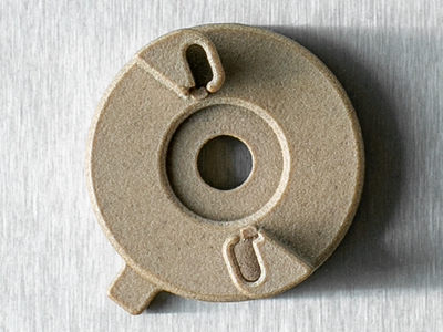
Kepstan® PEKK on SLS 3D Printing: Components for Semiconductor Manufacturing
In semiconductor manufacturing, components must withstand aggressive chemistries, high processing temperatures, and meet strict reliability standards. This article explores how PEKK SLS parts deliver these properties while minimizing warpage at elevated temperatures. We compare unfilled PEKK (PEKK-100) to common semiconductor materials, highlighting property data, processing considerations, and real-world relevance for semiconductor applications.
What is SLS 3D Printing?
Selective Laser Sintering (SLS) is an additive manufacturing process that uses a laser to fuse powdered material layer by layer. Unlike FDM or SLA, SLS does not require support structures, making it ideal for complex geometries.
Key benefits for semiconductor components include:
- Design freedom for intricate parts
- Excellent dimensional stability
- Ability to process high-performance polymers like PEKK
SLS is widely adopted in industries requiring precision and durability, such as aerospace, automotive, and now semiconductor manufacturing.
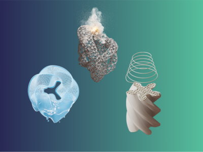
High-Performance Kepstan® PEKK Material
Kepstan® PEKK, developed by Arkema, belongs to the polyaryletherketone (PAEK) family. It offers:
- Exceptional chemical resistance
- High thermal stability (continuous use up to 260°C)
- Intrinsic flame retardancy (UL94 V-0)
- Excellent inherent FST (Flame, Smoke, Toxicity) properties
For SLS, PEKK powders provide low warpage, high mechanical strength, and dimensional accuracy, making them ideal for semiconductor environments where cleanliness and reliability are critical.
Alternative Materials in the Market
To meet strict requirements in semiconductor manufacturing, engineers increasingly turn to high-performance polymers such as:
- PEI (Polyetherimide)
- PEKK (Polyetherketoneketone)
- PEEK (Polyetheretherketone)
- PFA (Perfluoroalkoxy)
- PPS (Polyphenylene Sulfide)
Each offers a unique balance of thermal stability, chemical resistance, and mechanical strength, making them candidates for critical fab applications. However, PEKK stands out for its combination of processability in SLS, low warpage, and excellent performance under harsh conditions.
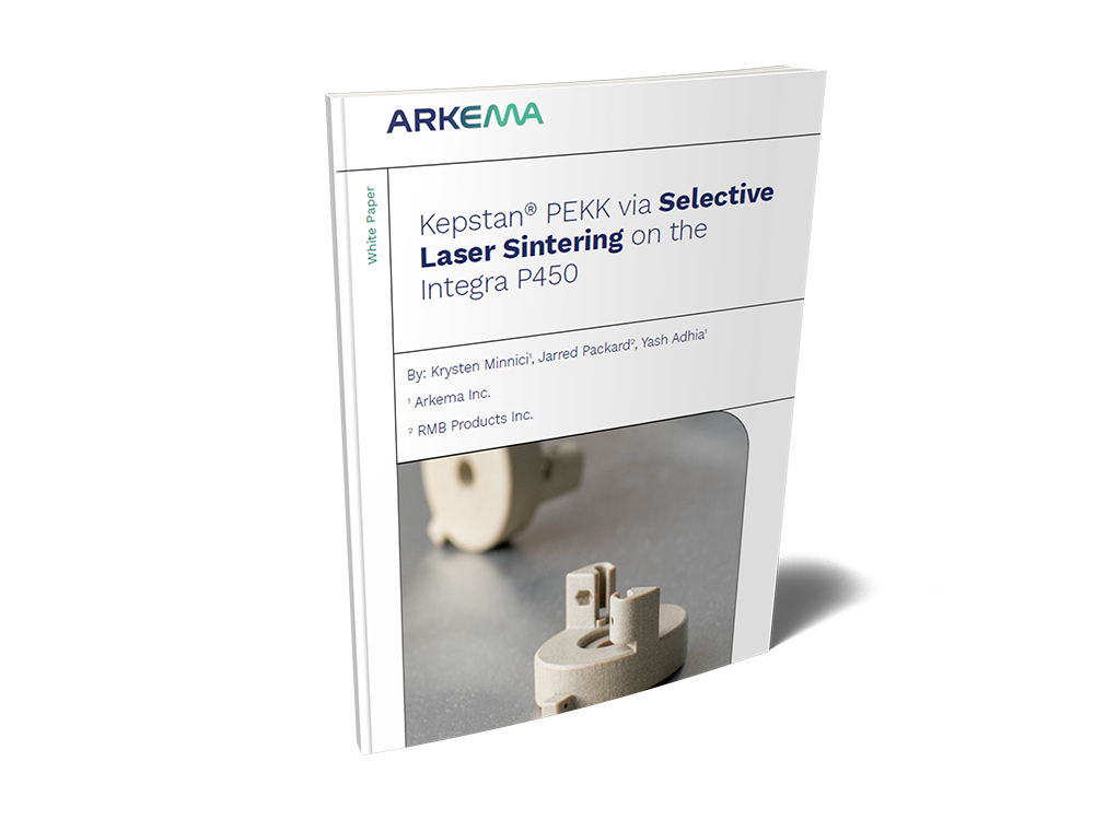
White Paper: Kepstan® PEKK via Selective Laser Sintering on the Integra P450
This white paper compares unfilled PEKK (PEKK-100) to common semiconductor materials, highlighting property data, processing considerations, and real-world relevance for semiconductor manufacturing.
For PEKK SLS, two main PEKK materials are available:
- PEKK-100 (Unfilled) – Launched in 2022 to meet demands for higher elongation at break, good insulation properties, and flame retardancy.
- HT-23 (Carbon-Filled) – Developed in 2018 for aerospace applications with Boeing, offering enhanced stiffness, dimensional stability, and low thermal expansion.
Both materials were developed in collaboration between EOS GmbH, Advanced Laser Materials (ALM), and Arkema, ensuring compatibility with industrial SLS systems.